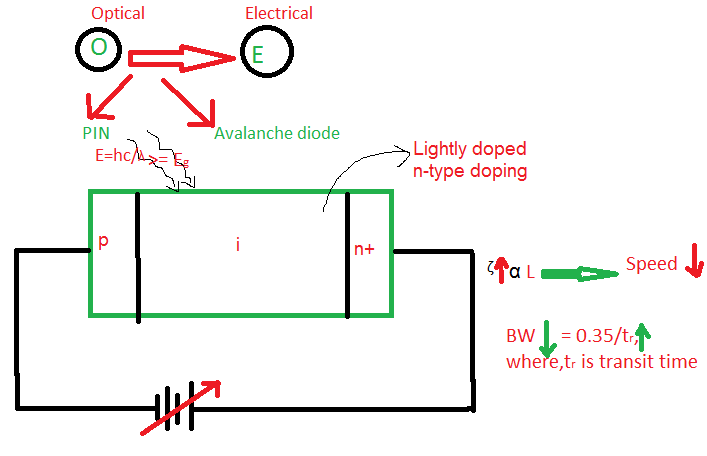
- Photo detector are used to provide optical to electrical conversion and always in Reverse Biased.
- Photo detectors are based on the principle of photo electric emission. in which if the energy of photons is greater than the band gap of the material the covalent bonds will be broken generating the free charge careers. E=hc/λ >=Eg
- Photo detectors are reverse biased so, that the depletion width can be increase and more number of photon can be collected by the detector.
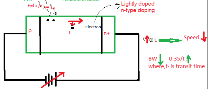
- In PIN Diode the intrinsic region is lightly doped(n), n-type region in order to collect more photons due to winding of depletion width.
- NOTE:-The depletion width or the Reverse biasing can not be increased s high as possible because the speed of response of device will reduce. Hence, there is compromise between the speed of the photo detector and Sensitivity.
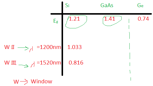
- Si and GaAs are not preferred for fabrication of photo detectors because the energy band gap is very high hence can not operate in window 2&3.
- Ge is also not preferred because the minority charge carries current very high which makes it thermally unstable. Ico(Ge0=Ico(Si)*10^3
- In avalanche photo diode the photo emission takes place due to impact ionization and Avalanche effect.
- The photo generated charge carrier are defined by an external potentials and they collide with more covalents bonds and due to the transfer of momentum covalents bonds are broken which results in to multiplication photons current.
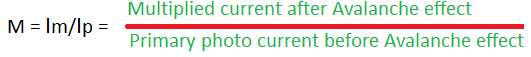
- Due to Impact ionization the primary photon current is multiplied hence, Avalanche photo diode can sensed weaker signal also.

